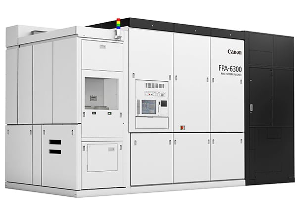
TOKYO, December 11, 2017—Canon Inc. announced today that the Company has commenced sales of a "200 mm option" for the FPA-5550iZ2 i-line1 and the FPA-6300ES6a KrF2 semiconductor lithography equipment, released in December 2016 and April 2012, respectively. These two systems are renowned for their ability to mass-produce logic, memory and image sensor devices required for IoT and automotive technologies.
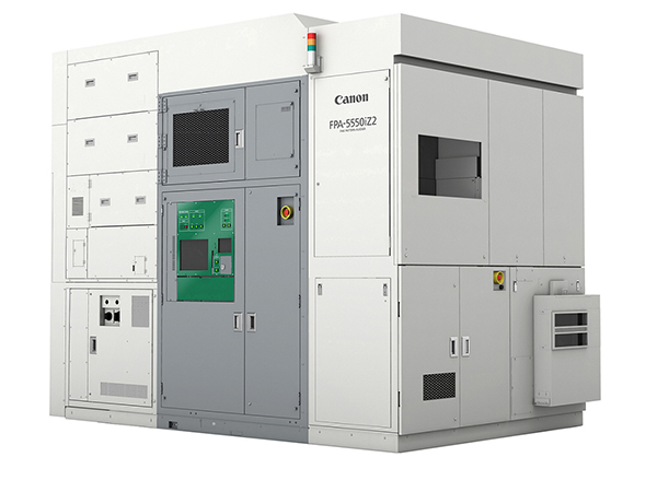
FPA-5550iZ2

FPA-6300ES6a
For the production of such semiconductor devices as those used in memory and microprocessors, manufacturing generally utilizes the latest in miniaturization technology and 300 mm wafers. However, due to the rapid expansion of the Internet of Things (IoT) and automotive devices, there is an increased demand for wide-variety small-lot production using existing processes and therefore a growing need among device makers for equipment capable of processing 200 mm wafers. Canon's FPA-5550iZ2 and FPA-6300ES6a semiconductor lithography equipment, which support 300 mm wafers, have been praised for their high productivity and overlay accuracy, and providing a new "200 mm option" enables Canon to meet a wide range of market needs.
When equipped with the "200 mm option," these systems achieve industry-leading3 200 mm wafer throughput rates in their class—230 wafers per hour4 for the FPA-5550iZ2 and 255 wafers per hour5 for the FPA-6300ES6a—contributing to reduced cost of ownership6.
Utilizing the same highly rated, trusted platform, both the FPA-5550iZ2 and FPA-6300ES6a allow for easy, continuous upgrades after purchase that provide a variety of solutions for models already in operation and increase productivity and overlay accuracy.
By continuing to provide a wide variety of solutions and upgrade options for its semiconductor lithography equipment, Canon supports users' increasing productivity needs.
- 1A semiconductor lithography system that utilizes a 365 nm wavelength mercury lamp as the light source. 1nm (nanometer) is 1 billionth of a meter.
- 2A semiconductor lithography system that utilizes a 248 nm exposure wavelength laser generated by combining the noble gas krypton (Kr) and the halogen gas fluoride (F).
- 3Among same-class i-line / KrF lithography systems. As of December 10, 2017, according to a Canon survey.
- 4The amount of 200 mm wafers exposed in one hour at 58 shots per wafer.
- 5The amount of 200 mm wafers exposed in one hour at 46 shots per wafer.
- 6Necessary equipment investments and operating costs related to semiconductor production. Used as one of the benchmarks for assessing the productivity of processes and production equipment used for semiconductor mass production lines.
